|
| The inner workings of Algorithm 127 |
|
Since the introduction of the SY77, there was this elusive, almost magical "free algorithm" aka Algorithm 127. Instead of using prefabricated operator stacks, this is said to allow creating your very own algorithm. But how?
Official information was only handed out with NDA, e.g., to the creators of C-Lab Polyframe. Mere mortals had to stare at the sysex dump with taunting parameters, yet no explanation.
You know the saying: When in doubt, read patents. And, dammit, we should've done this 30 years ago already ...
|
| Hello, operator? About this operator business. |
|
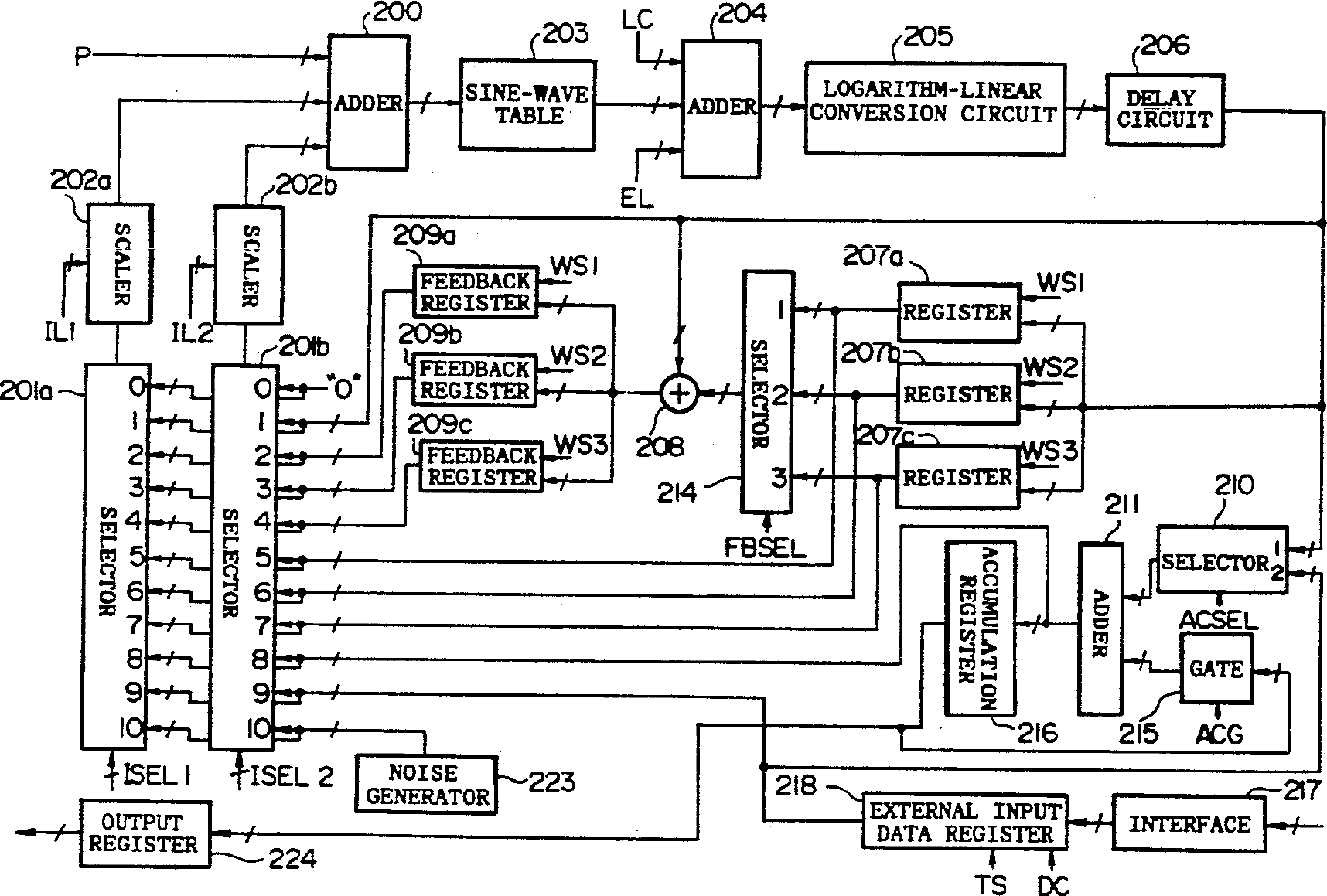
FM operator generator signal diagram
(Source: Patent US5076133)
The way the SY77/99 handles its operator stack does not differ conceptually from the DX7: the operator stack processing is strictly serialized, starting with Operator 6, then walking down the operators. On the SY77/99, the following steps are performed:
-
The operator's phase pointer is derived by adding (200) the optional phase offset P to up to two modulation sources (201a/b) which get scaled by the modulation index (202a/b) before adding. This indexes the log-sin table (203) and the result is scaled it with the operator volume offset and according operator envelope input (204) before converted to linear (205) and delayed to match the overall timing (206).
(Why log-sin, you ask? Because it saves on multiplications as log operator*amplitude = log operator + log amplitude.)
- In order to process an oscillator stack, we need to accumulate the generated output (211) with addition taking place on the direct or previous result (210) and the AWM2 input (215) — or none, of course. To preserve this value over the step-wise operator stack processing, the accumulator output is stored in the accumulator register (216).
As not all stacks are strictly linear — e.g. Operator 6 modulating Operators 5 and 4, see example below, we need a measure to store intermediate results. Feedback, in term, goes up the stack, not down. For this, three dedicated registers (207a/b/c) exist to store intermediate results. These also drive the feedback circuitry via the feedback selector (214), the feedback adder (208), and finally the according feedback register (209a/b/c) for storage.
(If you wondered why there is a maximum of three feedback loops, but only if there's no "oscillator forwarding" like from Op6 to Op4, now you now.)
-
Now the loop closes: we have all modulation sources in place (201a/b): no modulation, the direct operator output (from 206), the outputs of the three/each feedback (209a/b/c) and direct-storage (207a/b/c) registers, the accumulator (211), the external input (208), and a digital noise input (223).
- When we reach the algorithm stack's bottom, the accumulator output is fed into the output register (224).
Still there? Perfect. Because now you already have everything needed to understand the algorithm parameters in the MIDI implementation chart!
|
| What the MIDI implementation says |
|
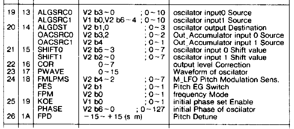
The algorithm parameters as listed in the MIDI specification
(Source: SY77 MIDI Specification)
Holding the above picture against the MIDI spec, makes it crystal clear:
-
ALGRSC0/1 refer to 201a/b and select the phase-modulating input. The values 0-10 provide the ISEL1/2 signals and hence directly correspond with the according inputs:
- 0: no modulation
- 1: forwarded operator output
- 2-4: Feedback register 1-3 (209a/b/c)
- 5-7: Storage register 1-3 (207a/b/c)
- 8: Accumulator output (211)
- 9: AWM2 input (218)
- 10: Noise generator (223)
-
SHIFT0/1 provide the scaling (202a/b) of ALGSRC0/1.
-
PHASE equals input P to the phase-index adder (200) and needs to be enabled by a dedicated KOE=1.
-
ALGDST routes the output to the according storage register 1-3 (207a/b/c) or, for 0, none.
As you notice from the signal flow, storage and feedback registers are directly coupled. If you write to a register, also the corresponding feedback register will be written to. Likewise, the feedback selector FBSEL will be set accordingly to either provide 0 or the output of the selected register.
OACSRC0 provides ACSEL to selector 210, either selecting zero (0), the current operator's output (1), or the external signal input (2). - Likewise, OACSRC1 provides ACG to gate 215, either selecting zero (0) or the accu register's (216) output.
|
| Building your own algorithm |
|
If you build your own algorithm, you need to keep the serialized operation in mind and which resources are required (or even preoccupied) for building the desired operator stack.
Let's have a look at Fig. 6 in the patent, showing the technical realization of Algorithm 33: Op3 is carrier, modulated by Op4, Op5, and Op6, while Op1, the second carrier, is only modulated by Op2. This leads to the following configuration:
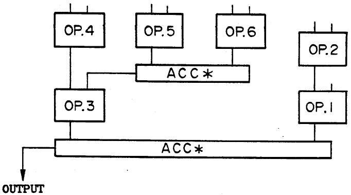
Algorithm 33 (Source: Patent US5076133)
- Op6 has no modulators (ALGSRC0/1=0) and outputs into the accumulator register (ACSEL/OACSRC0=1), the second summand is 0 (ACG/OACSRC1=0). The value is not stored in any other register (ALGDST=0)
- Op5 likewise outputs into the accumulator register, but with the second summand being the previously stored accumulator value (ACG/OACSRC1=1). Again, no further storage (ALGDST=0) and no modulators (ALGSRC0/1=0).
- Op4 also has no modulators (ALGSRC0/1=0), its value is just fed through w/o further storage are processing (OACSRC0/1=0, ALGDST=0).
- Op3 has two modulators, a forwarded Op4 result (ALGSRC0=1) and the accumulated value calculated from Op6 and Op5 (ALGSRC1=8). As it is part of the output signal, the value needs to be put into the accumulator (ACSEL/OACSRC0=1, AGC/OACSRC2=0).
- Op2 works like OP4.
- Op1 is just using one modulation input, i.e. the forwarding path of Op2 (ALGSRC0=1) and nothing (ALGSRC1=0). However, it forms the output together with Op3, so it takes the accu register feedback and adds it to the Op1 output (ACSEL/OACSRC0=1, AGC/OACSRC1=1).
- The internal chip logic will place the result into the output register.
Fig. 8 depicts Algorithm 41, which is slightly more complex.
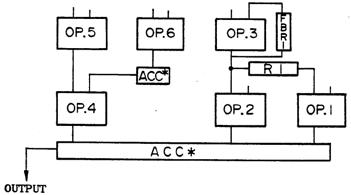
Algorithm 33 (Source: Patent US5076133)
- Again, you see the forwarding of Op6 to Op4 via the accumulator.
- As we have three carriers now, all of them need to be accumulated. For this reason, the accumulator will be occupied after Op4 for summing up the output.
- Consequently, the forwarding of Op3 to Op1 now needs a dedicated register (R1). This, however, is not wasted, as we need a feedback path from Op3 to itself anyway via the feedback register (FBR1).
- Finally, Op2 is modulated by Op3 with its output being summed into the accumulator. Likewise, Op1 is modulated via R1, and its output is also added into the accumulator.
Fig. 10 shows an elaborate configuration of, technically, Algorithm 32.
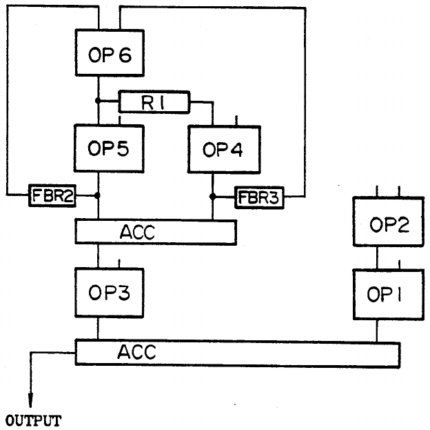
Algorithm 32 (Source: Patent US5076133)
We see that it is not the plain algorithm, but now with double feedback applied, hence occupying all three registers and feedback registers. What is nicely shown here is how the accumulator serves two purposes, first summing up Op5 and Op4, then the final output from Op3 and Op1. -
Here, the algorithm sheet in the user manual must be wrong, because it just makes no sense to delay Op6 for two cycles while waiting for Op5 and Op4 to finish. A more logical approach would be Op6→Op5→Op3←Op4 which is exactly what is depicted in Fig. 10.
Fig. 11 now shows a very special configuration of Algorithm 40.
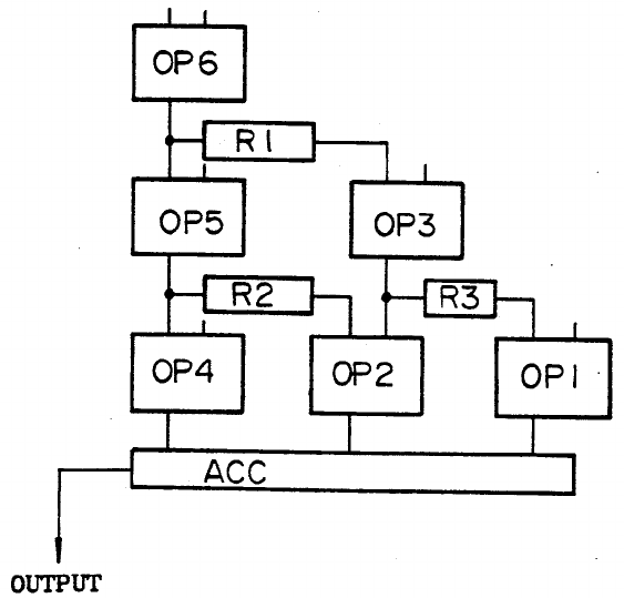
Algorithm 40 (Source: Patent US5076133)
This configuration has disabled feedback, but is modulating Op3 by Op6, Op2 by Op5, and Op1 by Op3. Resulting, all three registers are occupied, with the accumulator summing up the three carriers.
|
| Are you sure? |
|
Almost. It might be that Yamaha played switcheroo with the modulation source encoding.
Derek Cook did a fantastic DX7 to SY77 conversion guide and, as part of that work, also dived into the wonderful world of reverse-engineering sysex parameter settings.
Following his findings given in Annex A of his conversion guide, it seems that the AWM2/external input is 2, not 9, and consequently feedback registers, registers, and the accumulator output are shifted up one position.
|
|